2026
Co-first author
RowHammer and ColumnDisturb in 3D DRAM: New Vulnerability and Bitline Slice-Tracking Mitigation
K. Lee, F. G. Waqar, S. Cho, Z. Pan, S. Datta, and S. Yu.
IEEE International Electron Devices Meeting (IEDM), San Francisco, USA, 2026.
Abstract
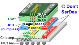
3D DRAM is a promising technology for sustaining DRAM scaling beyond the sub-10 nm node. However, its vertically integrated architecture introduces new dynamic disturbance mechanisms driven by wordline coupling and floating-body effects. This work establishes a device-to-system vulnerability analysis framework that uncovers a strong interaction between the RowHammer and ColumnDisturb phenomena. By comprehensively modeling all leakage mechanisms under realistic high-aspect-ratio etch process variations, we predict RowHammer and ColumnDisturb thresholds of approximately 57k and 120k activations, respectively—both significantly below the maximum activation count within a conventional 64 ms refresh window. To address this challenge, we propose a selector-based bitline slice-tracking mitigation scheme that reduces the counter area from 3% to 0.1% while effectively suppressing disturbance accumulation. Cycle-accurate Ramulator simulations show that the proposed approach provides reliable protection with less than 1% performance overhead, making it a practical solution for next-generation 3D DRAM systems.
Preprint
LLMET: Enabling Cross-Layer Evaluation Of Emerging M3D Memories For Energy-Efficient LLM Serving
M.-Y. Lee, H. Yang, F. G. Waqar, H. Simka, T. Krishna, M. Karim, and S. Yu.
arXiv preprint arXiv:2607.26491, 2026.
Abstract
The energy consumption of Large Language Model (LLM) serving is becoming a major system challenge as deployment scales, driven by hardware power and thermal constraints and rising electricity costs. A key contributor to chip energy dissipation is data movement between limited on-chip cache and off-chip High Bandwidth Memory (HBM). Meanwhile, emerging memory technologies such as monolithic 3D (M3D) integration of cache memories at the Back-End-Of-Line (BEOL) of logic chips enable larger and denser on-chip memories, creating new opportunities to reduce costly off-chip traffic. However, it remains unclear whether continuously scaling on-chip memory using emerging technologies can effectively improve the energy efficiency of LLM serving. To address this gap, we develop LLMET (LLM with Emerging Technology), a validated cross-layer simulation framework, and conduct a comprehensive study on the impact of large-capacity on-chip memory technologies across a broad range of models, applications and platforms. Utilizing M3D technology to expand the L2 cache from 40MB to 1GB yields a 44% reduction in chip energy during the Llama3.1-70B prefill phase with a 16K context window, based on LLMET simulation on a dual NVIDIA A100 GPU setup. On the 8x NVIDIA B200-like platform, extending the L2 cache from 128MB to 4GB saves the prefill energy by up to 24%. For the edge platform and workloads, the decode energy saving reaches 30% when increasing the 8MB cache size to 256MB. These results highlight the promise of ultra-large on-chip memories for energy-efficient LLM serving systems.
Preprint abstract
FAB Gain Cell Memory: A Folded Asymmetric Boosted Design To Improve Sense Margin For A Refresh-Free Operation
J. Sonawane, S. Deng, K. Lee, F. G. Waqar, C. Zhang, O. Phadke, S. Datta, and S. Yu.
IEEE Symposium on VLSI Technology and Circuits (VLSI), Hawaii, USA, 2026.
Abstract
We propose a folded asymmetric boosted 3T gain cell (GC) to enable a refresh-free, high-speed on-chip memory, using amorphous oxide semiconductor (AOS) FETs. An underlapped write FET suppresses write WL coupling, while an overlapped storage/read gating FET enables read WL driven storage node (SN) boosting through a preferential capacitive coupling. This boosting operation shifts the sensing operation out of the near-threshold regime, improving Vth variation tolerance. The measurements show a 1.48 V boosted memory window (at V_DD=1 V) and >300 s at 85 °C data retention (3 orders of improvement over conventional 3T GC). The projected 7nm FAB design shows 2.6 ns read delay and satisfies the refresh-free requirement for GPU last-level cache, given maximum data lifetime profiled from AI workloads.
Abstract source
First Demonstration Of Bit-Cost-Scalable And BEOL-Compatible Monolithic 4-Tier FeRAM Operating At 125 °C
E. Sarkar, J. Sonawane, H. Park, E. Quezada, K. Lee, D. Chakraborty, J. Shin, F. G. Waqar, C. Zhang,
H. J. Lee, M. Tian, S. Trolier McKinstry, V. Narayanan, A. I. Khan, S. Yu, and S. Datta.
IEEE Symposium on VLSI Technology and Circuits (VLSI), Hawaii, USA, 2026.
Abstract
We report the first experimental demonstration of a four-tier, bit-cost scalable (BiCS), back-end-of-line (BEOL) compatible monolithic 3D 1T1C Ferroelectric Random Access Memory (FeRAM), integrating 5 nm thin HZO ferroelectric capacitors with dual-gate Indium Gallium Oxide (IGO) access transistors. All tiers show uniform switching characteristics with 2P_r ≈ 60–70 μC/cm² and 2V_C ≅ 1.6–2.1 V. Refresh-free operation at 125 °C makes the technology ideal for monolithic stacking directly atop high-performance, power-intensive compute dies. We demonstrate successful read with write-back operations, 10-year data retention at 125 °C. Benchmarking projections indicate that this BiCS-based approach enables aggressive density scaling, potentially reaching 4.36 Gb/mm² for a 100-tier stack.
Abstract source
Co-first author
Workload-Derived AC Bias Temperature Instability And Mechanism Contributions In BEOL Oxide Channel DRAM Access Transistors
H. J. Lee, F. G. Waqar, H. Park, C. Zhang, J. Shin, E. Sarkar, H. Kim, C. Im, M. J. Hong, D. Ha,
A. I. Khan, S. Yu, and S. Datta.
IEEE Symposium on VLSI Technology and Circuits (VLSI), Hawaii, USA, 2026.
Abstract
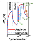
This work presents a workload-driven bias temperature instability (BTI) modeling framework that translates execution-based DRAM row-access traces (derived from Ramulator) into time-resolved AC-BTI waveforms for back-end-of-line (BEOL) oxide channel FETs. By mapping AC-to-DC BTI degradation within a single time window, threshold voltage (Vth) evolution is tracked without hidden recovery. This enables physics-based identification of BTI mechanisms based on their time-exponents. Our framework resolves workload-dependent relative contributions of competing mechanisms, enabling reliable BTI projection and workload-aware controller design guidance.
Abstract source
First author
Enabling Context-Switchable Monolithic 3D FPGA Design Using Bistable Ferroelectric Inverters
F. G. Waqar, M. Chen, Z. He, Z. Wan, M. Shon, W.-H. Huang, J. Cong, and S. Yu.
IEEE International Symposium on Field-Programmable Custom Computing Machines (FCCM), Atlanta, GA, 2026.
Abstract
This work proposes a time-multiplexed, non-volatile FPGA design based on back-end-of-line (BEOL) compatible ferroelectric field-effect transistors (FeFETs) for low-power edge acceleration. In battery-constrained microrobotic applications targeting localization and odometry, we show that a power-gateable reconfigurable FPGA can save >50% of on-board resources and improve cumulative localization error, system power, and FPS by 75% over a baseline single-pipeline deployment, and by 25–35% over existing partial-reconfiguration techniques. Using an FeFET as the storage element in a bistable, high-gain inverting topology, the fabric targets ultra-low standby power while improving programmable-mesh density and critical latency. Through integration of bistability using a virtual rail, we demonstrate 3.74–12.5× lower standby power and non-volatility that enables power gating while maintaining sub-ns context-switching time at the cell level. Using the latest Verilog-to-Routing (VTR) flow integrated with experimentally calibrated BSIM+Preisach SPICE models, we evaluate and compare monolithic 3D (M3D) proposals at tile- and system-level integration of a 4-configuration bit-cell on Koios deep-learning benchmarks in the 7 nm technology node with 34 % improvement in density over a single-configuration conventional FPGA and 40% improvement in area-delay-squared (AT²) product.
Abstract source
Presentation only
Non-Volatile FPGAs And CIM Enabled By Dual-FeFET Memory In 28 nm Foundry Process
M. Chen, F. G. Waqar, J. Jia, V. Garg, and S. Yu.
MADCAP Workshop at IEEE FCCM, Atlanta, GA, 2026.
Radiation Reliability Of BEOL-Compatible Ga-Doped Indium Oxide MOSFETs For eDRAM Applications
S. G. Kirtania, C. Zhang, S. E. Wodzro, F. G. Waqar, H. J. Lee, D. Chakraborty, J. D. Yeager,
D. E. Wolfe, A. I. Khan, S. Yu, and S. Datta.
IEEE International Reliability Physics Symposium (IRPS), Tucson, AZ, 2026.
Abstract
This work addresses a key bottleneck in radiation-hardened computing: achieving high-density embedded memory in monolithically stacked (M3D) systems without relying on area-inefficient SRAM or radiation-sensitive scaled Si access devices. We evaluate back-end-of-the-line (BEOL) compatible Ga-doped indium oxide (IGO) MOSFETs as access transistors for vertically integrated 1T-1C embedded DRAM (eDRAM) under both ionizing and displacement-damage radiation. Devices are subjected to ⁶⁰Co gamma total-ionizing-dose (γ-TID) up to 10 MRad(air) and neutron fluence up to 10¹⁵ n/cm². IGO MOSFETs exhibit exceptional γ-TID tolerance: transfer characteristics, threshold voltage (V_th), and effective mobility remain statistically invariant up to 10 MRad, and sub-gap density-of-states (DOS) extraction from multi-frequency CV confirms negligible ionization-induced defect generation. In contrast, neutron irradiation produces pronounced displacement damage, manifested as positive V_th shifts, mobility degradation, and increased mid-gap and band-tail defect densities. Bias-temperature-instability (BTI) measurements show radiation-accelerated parameter drift; enhanced PBTI is consistent with activation of deep traps in the HfO₂ gate dielectric, while increased NBTI is consistent with radiation-assisted hydrogen diffusion. Calibrated TCAD reproduces these trends, linking γ-TID primarily to modest interface-state increases and neutrons to broader/deeper defect spectra. System-level analysis indicates IGO-based 1T-1C eDRAM achieves ~500× higher retention than silicon baselines and only a 2% retention penalty at 10 MRad (vs ~42% for Si FinFETs), positioning BEOL IGO as a scalable access-device platform for dense, radiation-hardened monolithic eDRAM.
Abstract source
Omelet: A Packaging-Aware Hierarchical Interconnect Simulator For 2.5D/3D Chiplet Architectures
J. Kim, D. Baig, F. G. Waqar, A. Victor, S. Yu, M. S. Bakir, and C. Hao.
ACM/IEEE International Symposium on Computer Architecture (ISCA), Raleigh, NC, 2026.
Abstract
Monolithic integration of SoCs is reaching practical and economic limits, motivating the transition to disaggregated chiplet-based 2.5D/3D systems. In these systems, system performance depends not only on microarchitecture, but is tightly coupled to integration decisions such as stacking, interposers, and bonding methods. These packaging decisions directly shape communication characteristics, including link latency, bandwidth, energy, and I/O density. At the same time, communication is no longer confined to a uniform on-chip network. Instead, data movement traverses multiple interconnect domains, including on-chip wires, lateral interposer links, and vertical die-to-die connections. Since each domain is implemented using different physical technologies, they exhibit distinct electrical and communication characteristics, naturally forming a hierarchical interconnect structure. However, existing simulators rely on packaging-agnostic, decoupled abstractions that fail to capture technology-specific link behavior and cross-layer interactions. This disconnect obscures integration-driven bottlenecks and limits accurate system-level design space exploration. We present Omelet, a packaging-aware hierarchical interconnect simulator for 2.5D/3D chiplet systems. The simulator integrates intra-chiplet networks (Network-on-Chip, NoC), interposer-level communication (Network-on-Interposer, NoI), and vertical tier-to-tier links (Network-on-Layer, NoL) within a unified cycle-level framework, with link parameters derived from electromagnetic extraction and compact SPICE models of advanced packaging interconnects. This unified hierarchy enables architects to evaluate how packaging technologies, network architectures, and chiplet organizations jointly influence latency, congestion, and bottleneck formation in multi-chiplet 2.5D/3D systems.
Abstract source
2025
Co-first author
Demonstration Of 3T0C Gain Cells With Self-Aligned Oxide Transistors For Parasitic-Aware Design At Array-Level
S. Deng, J. Sonawane, F. G. Waqar, O. Phadke, C. Zhang, M.-Y. Lee, S. Yu, and S. Datta.
IEEE International Electron Devices Meeting (IEDM), San Francisco, USA, 2025.
Abstract
Capacitorless gain-cell (GC) memories realized with amorphous oxide semiconductor (AOS) devices promise cache-class speed with higher density. However, AOS transistors typically adopt gate-to-source/drain overlaps (OLs), introducing high parasitics that degrade speed, density, and energy efficiency at the array level. In this work, we performed a comparative study of parasitic effects in GCs using overlapped (OL) and self-aligned (SA) AOS transistors as testbeds. To eliminate WWL-SN capacitance coupling and other inherent issues in 2T0C configurations, we experimentally demonstrated 3T0C GCs with SA transistors, achieving negligible voltage drop at storage node, a 10× improvement in retention, and a 4.3× speed boost at iso-leakage compared to OL counterparts. Cycle-accurate system analysis indicates that GPU caches using SA 3T0C GCs can reduce the energy-delay-area product by 75-80% while doubling capacity over SRAM within a single BEOL memory tier. These findings provide useful parasitic-aware GC design guidelines at the array level.
Abstract source
First author
Best presentation
CMOS+X: Stacking Persistent Embedded Memories Based On Oxide Transistors Upon GPGPU Platforms
F. G. Waqar, M.-Y. Lee, S. Yoon, S. Lim, and S. Yu.
ACM/IEEE International Symposium on Memory Systems (MEMSYS), Washington DC, 2025.
Abstract
In contemporary general-purpose graphics processing units (GPGPUs), the continued increase in raw arithmetic throughput is constrained by the capabilities of the register file (single-cycle) and last-level cache (high bandwidth), which require the delivery of operands at a cadence demanded by wide single-instruction multiple-data (SIMD) lanes. Enhancing the capacity, density, or bandwidth of these memories can unlock substantial performance gains; however, the recent stagnation of SRAM bit-cell scaling leads to inequivalent losses in compute density. To address the challenges posed by SRAM's scaling and leakage power consumption, this paper explores the potential CMOS+X integration of amorphous oxide semiconductor (AOS) transistors in capacitive, persistent memory topologies (e.g., 1T1C eDRAM, 2T0C/3T0C Gain Cell) as alternative cells in multi-ported and high-bandwidth banked GPGPU memories. A detailed study of the density and energy tradeoffs of back-end-of-line (BEOL) integrated memories utilizing monolithic 3D (M3D)-integrated multiplexed arrays is conducted, while accounting for the macro-level limitations of integrating AOS candidate structures proposed by the device community (an aspect often overlooked in prior work). By exploiting the short lifetime of register operands, we propose a multi-ported AOS gain-cell capable of delivering 3x the read ports in ~76% of the footprint of SRAM with over 70% lower standby power, enabling enhancements to compute capacity, such as larger warp sizes or processor counts. Benchmarks run on a validated NVIDIA Ampere-class GPU model, using a modified version of Accel-Sim, demonstrate improvements of up to 5.2x the performance per watt and an average 8% higher geometric mean instruction per cycle (IPC) on various compute- and memory-bound tasks.
Preprint abstract
First author
Monolithic 3D FPGA Design And Synthesis With Back-End-Of-Line Configuration Memories
F. G. Waqar, J. Zhang, A. Lu, Z. He, J. Cong, and S. Yu.
ACM/IEEE Design Automation Conference (DAC), San Francisco, CA, 2025.
Abstract
This work presents a novel monolithic 3D (M3D) FPGA architecture that leverages stackable back-end-of-line (BEOL) transistors to implement configuration memory and pass gates, significantly improving area, latency, and power efficiency. By integrating n-type (W-doped In₂O₃) and p-type (SnO) amorphous oxide semiconductor (AOS) transistors in the BEOL, Si SRAM configuration bits are substituted with a less leaky equivalent that can be programmed at logic-compatible voltages. BEOL-compatible AOS transistors are currently under extensive research and development in the device community, with investment by leading foundries, from which reported data is used to develop robust physics-based models in TCAD that enable circuit design. The use of AOS pass gates reduces the overhead of reconfigurable circuits by mapping FPGA switch block (SB) and connection block (CB) matrices above configurable logic blocks (CLBs), thereby increasing the proximity of logic elements and reducing latency. By interfacing with the latest Verilog-to-Routing (VTR) suite, an AOS-based M3D FPGA design implemented in 7 nm technology is demonstrated with 3.4x lower area-time squared product (AT²), 27% lower critical path latency, and 26% lower reconfigurable routing block power on benchmarks including hyperdimensional computing and large language models (LLMs).
Preprint abstract
Digital Compute-In-Memory Ising Annealer With Ferroelectric Capacitor-Based nvSRAM For Combinatorial Optimization Problems
Y. Kong, J. Jia, A. Lu, F. G. Waqar, Y.-C. Luo, H. Li, I. Young, and S. Yu.
IEEE International Symposium on Circuits and Systems (ISCAS), London, UK, 2025.
Abstract
Combinatorial optimization problems (COPs) have a wide range of applications. The Ising model-based annealer is gaining attention for its efficiency and speed in finding approximate solutions. However, building an Ising machine that is area- and energy-efficient, scalable, and with low compute latency in CMOS is challenging. In this paper, we present a digital compute-in-memory (DCIM) Ising annealer that uses ferroelectric capacitor (FeCap)-based nvSRAM to solve COPs like the Traveling Salesman Problem (TSP). By using weak recall operations, our design eliminates the need to reload weights, significantly reducing energy consumption and speeding up processing compared to other approaches. Simulations using a 16nm PDK demonstrate that our nvSRAM-based DCIM array maintains accuracy while reducing latency by up to 55.0% and energy by 49.6% compared to prior work implemented with conventional SRAM DCIM array. Algorithm validation further shows that the random noise introduced by weak recall can be effectively utilized in the annealing process.
Abstract source
Presentation only
Digital Compute-In-Memory Ising Annealer With Ferroelectric Capacitor-Based nvSRAM For Travelling Salesman Problem
Y. Kong, J. Jia, A. Lu, F. G. Waqar, Y.-C. Luo, H. Li, I. Young, and S. Yu.
International Workshop on Ising Machines (IISM), Chicago, IL, 2025.
Hardware Acceleration Of Kolmogorov-Arnold Network (KAN) For Lightweight Edge Inference
W.-H. Huang, J. Jia, Y. Kong, F. Waqar, T.-H. Wen, M.-F. Chang, and S. Yu.
ACM/IEEE Asia and South Pacific Design Automation Conference (ASP-DAC), Tokyo, Japan, 2025.
Abstract
Recently, a novel model named Kolmogorov-Arnold Networks (KAN) has been proposed with the potential to achieve the functionality of traditional deep neural networks (DNNs) using orders of magnitude fewer parameters by parameterized B-spline functions with trainable coefficients. However, the B-spline functions in KAN present new challenges for hardware acceleration. Evaluating the B-spline functions can be performed by using look-up tables (LUTs) to directly map the B-spline functions, thereby reducing computational resource requirements. However, this method still requires substantial circuit resources (LUTs, MUXs, decoders, etc.). For the first time, this paper employs an algorithm-hardware co-design methodology to accelerate KAN. The proposed algorithm-level techniques include Alignment-Symmetry and PowerGap KAN hardware aware quantization, KAN sparsity aware mapping strategy, and circuit-level techniques include N:1 Time Modulation Dynamic Voltage input generator with analog-CIM (ACIM) circuits. The impact of non-ideal effects, such as partial sum errors caused by the process variations, has been evaluated with the statistics measured from the TSMC 22nm RRAM-ACIM prototype chips. With the best searched hyperparameters of KAN and the optimized circuits implemented in 22 nm node, we can reduce hardware area by 41.78x, energy by 77.97x with 3.03% accuracy boost compared to the traditional DNN hardware.
Preprint abstract
Radiation-Resilient Amorphous Indium Oxide FeFETs For Embedded Nonvolatile Memory
S. G. Kirtania, F. G. Waqar, D. Chakraborty, J. Shin, E. Sarkar, J. Reiss, D. E. Wolfe, S. Yu, and S. Datta.
IEEE International Reliability Physics Symposium (IRPS), Monterey, CA, 2025.
Abstract
We report the first-ever study on the radiation resilience of a back-end-of-line (BEOL) compatible W-doped Indium Oxide (IWO) ferroelectric field-effect transistor (FEFET) under neutron irradiation. The findings demonstrate remarkable resilience of both Hf₀.₅Zr₀.₅O₂ (HZO) ferroelectric capacitors (FECAPs) and IWO FEFETs to neutron irradiation. Subjected to neutron irradiation at fluences up to 10¹⁵ n/cm², HZO FECAPs maintain stable remnant polarization (2Pr) and coercive voltage (2Vc) up to 10¹¹ cycles without any breakdown. The IWO FEFETs show robust switching performance and exhibit minimal degradation in memory window (MW) and read current window (CW). Importantly, the retention and endurance performance remain stable after neutron radiation exposure, without significant failure. Destiny simulations were performed to assess the impact of radiation on the system-level performance of an 8 MB 1T-1FEFET-based embedded RAM at the 32 nm node. The results showed negligible effects on read latency and only a minor 0.36% increase in dynamic read energy at a neutron fluence of 10¹⁵ n/cm². The combination of high performance, non-volatility, and radiation hardness makes IWO FEFETs a promising candidate for high-density, persistent memory applications in radiation-rich environments.
Abstract source
Presentation only
Experimental Demonstration Of Gain Cells With Self-Aligned Oxide Transistors For Reduced Capacitive Coupling
J. Sonawane, S. Deng, F. G. Waqar, O. Phadke, C. Zhang, M.-Y. Lee, S. Datta, and S. Yu.
IEEE Non-Volatile Memory Technology Symposium (NVMTS), Atlanta, GA, 2025.
2024
First Demonstration Of W-Doped In2O3 Gate-All-Around (GAA) Nanosheet FET With Improved Performance And Record Threshold Voltage Stability
E. Sarkar, C. Zhang, D. Chakraborty, F. Waqar, S. Kirtania, K. A. Aabrar, H. Park, J. Shin, M. Tian,
A. I. Khan, S. Yu, and S. Datta.
IEEE International Electron Devices Meeting (IEDM), San Francisco, USA, 2024.
Abstract
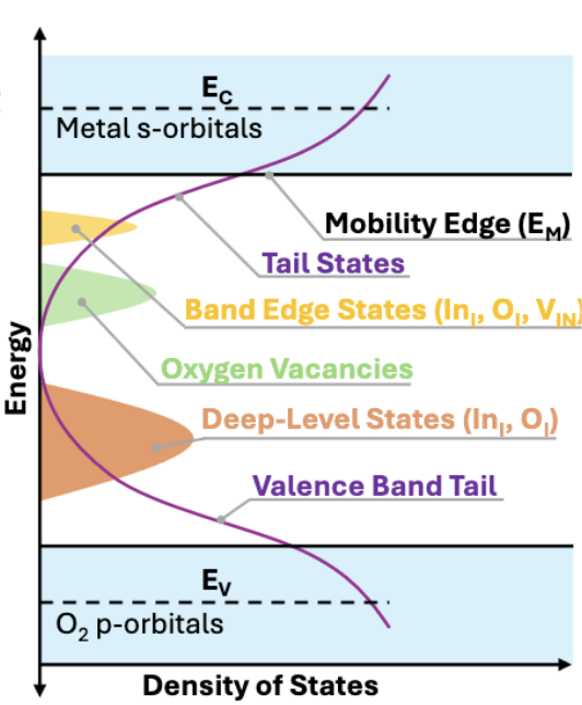
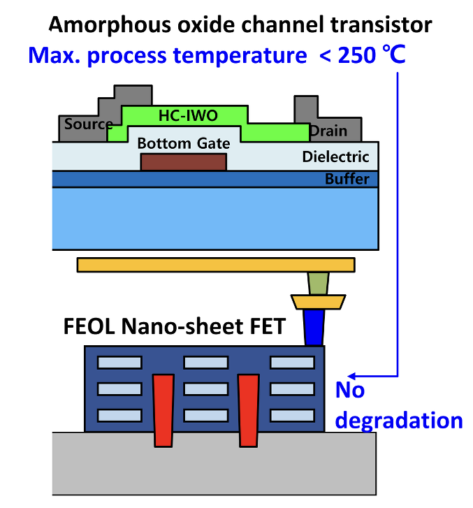
We demonstrate a gate-all-around (GAA) nanosheet FET using an atomic layer deposited (ALD) tungsten (W) doped indium oxide (In₂O₃) or IWO channel. We developed a novel channel release process with a metal sacrificial layer (SL), that enables lithography-independent definition of the device channel length (LCh). The fabricated nanosheet FETs with scaled dimensions of LCh=50nm and WNanosheet=30nm demonstrate high on-state current (ION) of 815 μA/μm for VDD=1V, VG-VT=3.5V with an off-state current (IOFF) of 4 nA/um at VG=VT-1V. These GAA nanosheet IWO FETs showcase record high bias stress stability with threshold voltage (VT) shift of only 88mV for stress voltage VG- VT=2.6V (stress field, Eox=Vov/EOT=22 MV/cm). The high I_ON of GAA nanosheet FET, along with its BEOL compatibility, enables access transistors for 3D stacked embedded MRAM, with peripheral CMOS under the array, consequently improving the cell density by 3.4x compared to conventional MRAM with front-end-of-line (FEOL) access transistors.
Abstract source
Amorphous Indium Oxide Channel FeFETs With Write Voltage Of 0.9 V And Endurance > 1012 For Refresh-Free 1T-1FeFET Embedded Memory
S. G. Kirtania, O. Phadke, E. Sarker, K. A. Aabrar, D. Chakraborty, F. Waqar, S. Jaewon, T. Pantha,
S. Dutta, A. I. Khan, S. Yu, and S. Datta.
IEEE International Electron Devices Meeting (IEDM), San Francisco, USA, 2024.
Abstract
For the first time, we demonstrate a back end of the line (BEOL) compatible amorphous oxide semiconductor (AOS) FeFET with a record-low operating voltage <0.9 V and write-speed of 20ns while maintaining a current window (I_LVT/I_HVT) > 10³. We also demonstrate a) bipolar write endurance reaching 10¹² cycles (measured), b) fast read speed of 50 ns, c) read endurance greater than 10¹² cycles, and d) retention time exceeding 10⁴ seconds at 85°C. Array level analysis of AOS 1T-1FeFET offers 100x less standby power than 2T eDRAM and 1,000x lower refresh power than eMRAM due to non-destructive read and comparable write speed due to faster switching. AOS channel FeFETs a potential candidate for high density embedded memory in scaled CMOS technology nodes.
Abstract source
2023
Presentation only
A Tutorial On The Bayesian Approach To Inverse Problems (Eg, In Heat Transfer)
F. Waqar, S. Patel, and C. Simon.
AIChE Annual Meeting, 2023.
2020
Towards Explainable Message Passing Networks For Predicting Carbon Dioxide Adsorption In Metal-Organic Frameworks
A. Raza, F. Waqar, A. Sturluson, C. Simon, and X. Fern.
ML4Molecules Workshop at NeurIPS, 2020. arXiv:2012.03723.
Abstract
Metal-organic framework (MOFs) are nanoporous materials that could be used to capture carbon dioxide from the exhaust gas of fossil fuel power plants to mitigate climate change. In this work, we design and train a message passing neural network (MPNN) to predict simulated CO₂ adsorption in MOFs. Towards providing insights into what substructures of the MOFs are important for the prediction, we introduce a soft attention mechanism into the readout function that quantifies the contributions of the node representations towards the graph representations. We investigate different mechanisms for sparse attention to ensure only the most relevant substructures are identified.
Preprint abstract